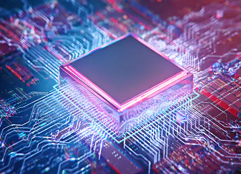
Semiconductor
Central components of digital devices
Semiconductor applications – the heart of modern technologies
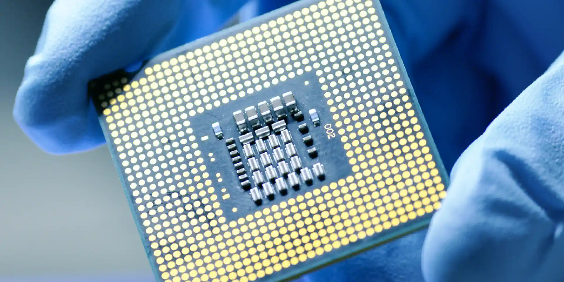
“Without semiconductors there wouldn’t be any microchips, and without microchips there wouldn’t be a digital world.” Microchips are a vital component of all digital systems. By processing and storing information, they ensure that electronic devices do what they’re supposed to. Specific optical-chemical processes can be used to produce tiny integrated circuit structures on microchips that rapidly process and transmit electrical signals. These small computer chips are based on semiconductors.
Solutions for asphericon’s semiconductor technology
- High-performance optical coatings with unsurpassed reflective properties
- High-end finishes for optics with low roughness in the Angstrom range
- Customized mirrors of unmatched quality
- Freeform surface systems or aspherical lenses for high-performance cameras used in wafer inspection
- Aspherical cylinders and BeamTuning products for effective, flawless laser guidance in wafer production
Materials for semiconductors
Probably the best-known material used to make semiconductors is silicon. It’s no surprise that after Gordon Teal, the pioneer from Texas Instruments, announced the creation of the first commercial silicon transistor back in 1954, the period since then has become known as the Silicon Age. Silicon is an ideal semiconductor as it combines unbeaten characteristics for use in microelectronics and nanoelectronics. It therefore quickly became the material of choice for making electronic devices and paved the way for their miniaturization and performance improvements. Other materials which are often used as semiconductors because of their high energy resolution, absorption capacity and drift speed are germanium, gallium arsenide and indium phosphide.
The many uses of semiconductor materials
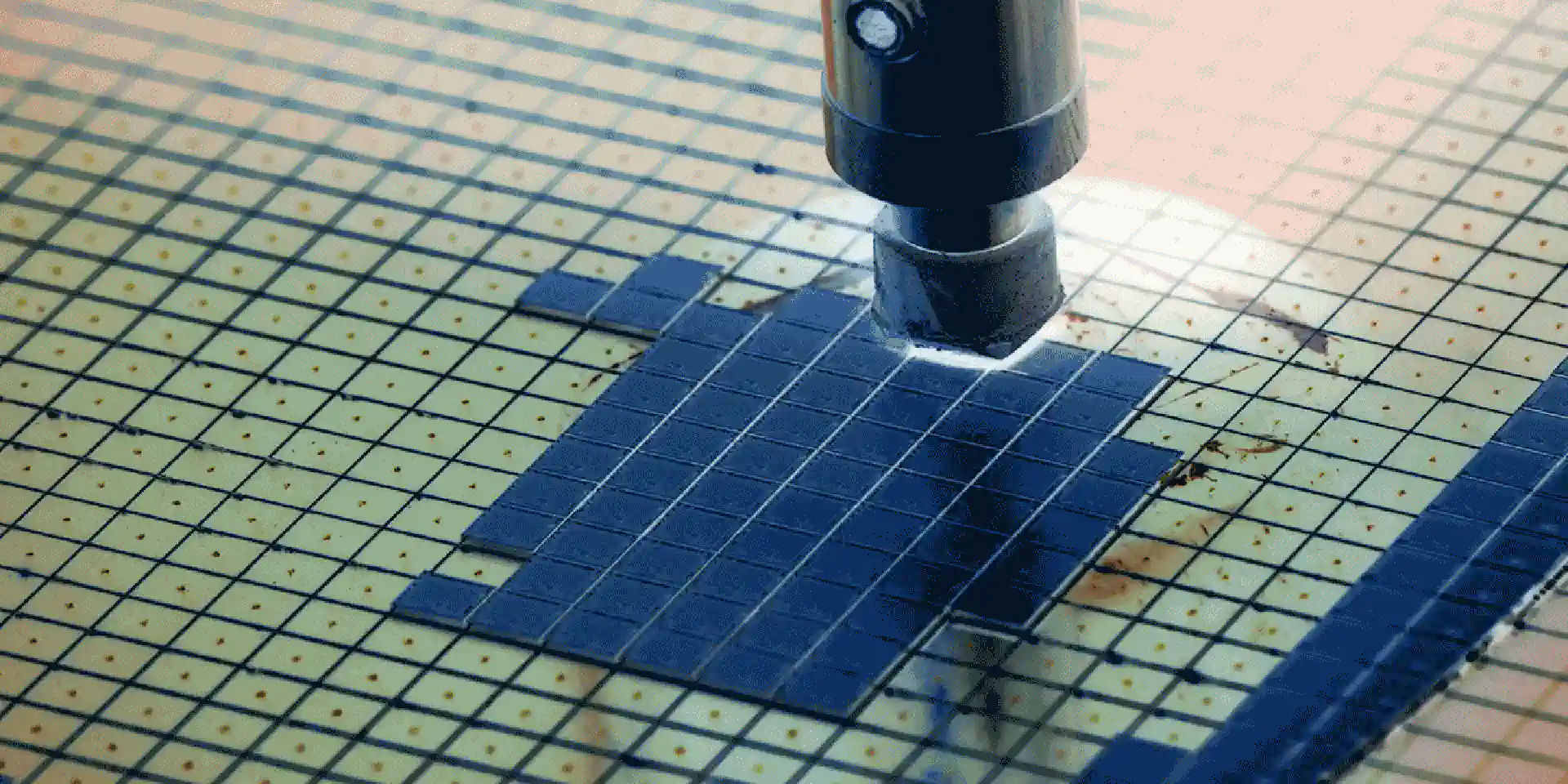
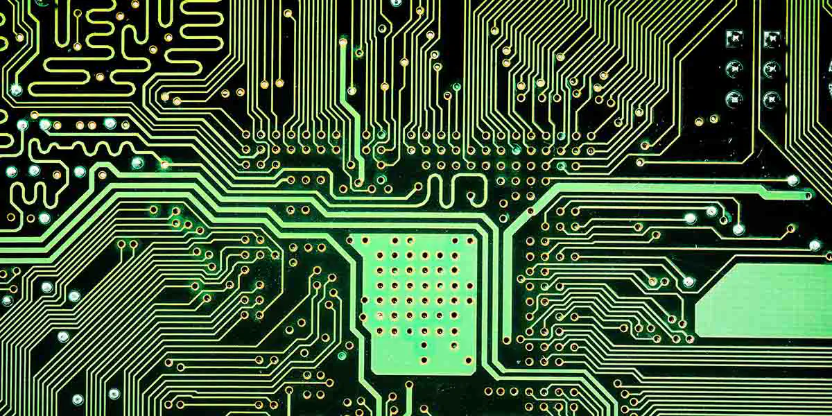
Semiconductors are used in many types of advanced applications; indeed, countless developments would be impossible without them. Semiconductor technology is the umbrella term for the production of microelectronic components. Under certain conditions, semiconductors can act as conductors or insulators, making them suitable for all sorts of applications. Using thin-film technology, extremely thin layers of a wide variety of materials (including metallic, dielectric and semiconducting materials) can be produced on a carrier substrate (e.g. silicon wafers). They are then structured and etched using photolithographic processes. This results in different layers with a thickness of just a few micrometres or even nanometres, which together form an integrated circuit on a semiconductor component.
Large volumes of semiconductor materials are to be found above all in microsystems technology, which particularly includes sensors and data processing (such as microchips, integrated circuits, transistors, etc.). In addition, they’re also used in solar technology (solar cells), consumer electronics (mobile phones, game consoles, refrigerators), and for lighting and imaging tasks (light, LED and OLED displays).

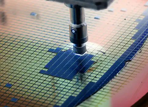
Producing high-quality silicon wafers
By means of the Czochralski method, a high-purity silicon is melted under constant rotation while being pulled upwards. Crystallization leads to the formation of cylindrical ingots or seed crystals consisting of monocrystalline silicon. These seed crystals are later cut into thin slices and form the basis for all kinds of electrical components. Although silicon has long been cut by sawing it with a diamond blade, this mechanical intervention damages the material and causes process shortcomings.
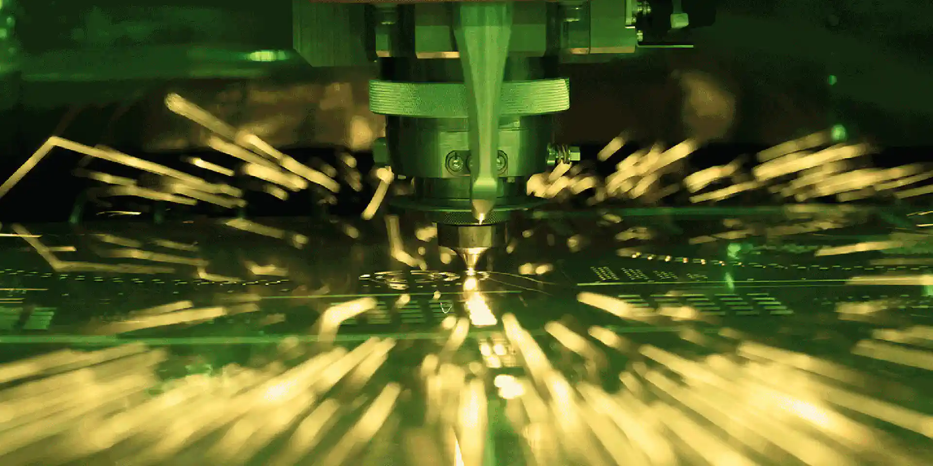
By contrast, laser cutting is much more efficient and causes much less damage. It doesn’t cause any mechanical wear and therefore allows consistent cutting quality. Furthermore, microcracks on the cut edges are significantly reduced, preventing wafer breakage. With the aid of a point-shaped or linear tool, laser cutting enables not only a narrower cutting width but also greater two-dimensional flexibility. Apart from laser cutting, laser light – a much-used tool – is also used to mark wafers.