Wafer Inspection
Camera systems for controlling microchip components
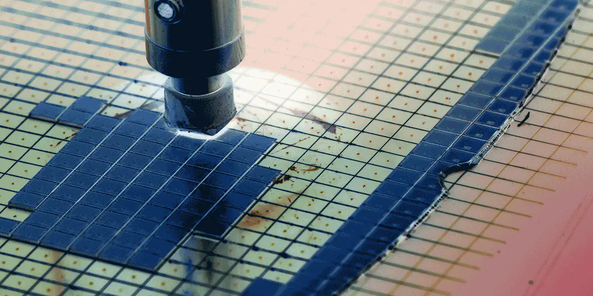
With the help of high-quality camera systems, it is possible to inspect the surfaces of wafers and detect the smallest deviations from the optimum surface. Wafers are square or circular thin disks that serve as a base plate for the deposition of electronic components. Wafers are used in various areas, e.g. in photovoltaics, micromechanics and the semiconductor industry. The requirements for wafer inspections are very high, as extremely detailed measurements of wafer microstructures down to the nanometer range have to be generated. In addition, very precise control of the UV radiation and the associated correct selection of the wavelength is extremely important in order to achieve ideal measurement results.
High demands on production and results
Due to technical progress and intensive research work, the electronic components installed on wafers and the resulting products (e.g. microchips) are constantly growing. The increasing complexity and density of the structures associated with this makes resolution more difficult. State-of-the-art camera systems, which are used for quality control of wafers, have to meet these high requirements from year to year. Only in this way can unevenness, (micro)cracks, humps or coating defects be reliably detected during inspection of the wafer material or its surface and displayed on a screen.
(Freeform) systems for high-performance cameras
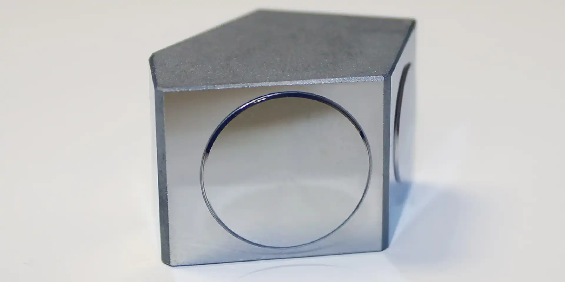
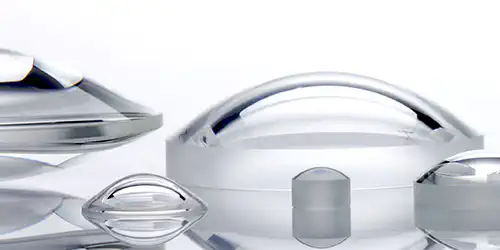
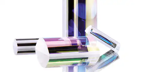
High-quality optical components form the basis for high-performance camera systems. The best imaging results can be achieved, for example, with freeform surface systems or aspherical lenses. Pin sharp details, compensation of spherical aberration and precise measurements can be achieved with aspheric lenses or freeforms from asphericon. According to your requirements, the production of individual UV-VIS lenses for an effective quality assurance of your wafer inspection systems is easily possible. Reliable process monitoring can thus be guaranteed even with simultaneously high wafer throughput rates. Thermal as well as mechanical test procedures of our in-house environmental tests fully confirm the high quality of our products.
asphericon's optical elements and systems guarantee the highest imaging quality and complement your optical systems to your complete satisfaction. Defective products can be reliably detected and sorted out for a smooth inspection process.
Selected product and service highlights