Optical Lithography
Optical layers for complex information structures on wafers
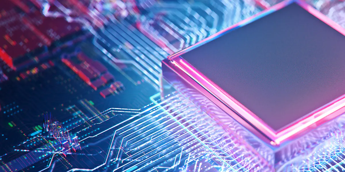
Optical lithography is a key technology in semiconductor and microsystems technology. Whether mobile phone, computer or car, the functionality of our everyday technical companions is based on the technology of lithography. The application of complex micro- and nanostructures on wafers forms the basis for the core component of all technical devices, which is the microchip.
Wafer structuring process
Lithography thus describes the process of structuring wafers. In the case of microchip production, wafers are pure silicon wafers on which a radiation-sensitive film is first applied, usually a special photoresist layer. An image of a photomask is transferred to the radiation-sensitive photoresist by means of exposure. Depending on the process, the exposed or unexposed areas are resolved, resulting in a lithographic mask. The resulting structures and further physical and chemical processing steps, e.g. special etching processes, result in complex circuits.
Factors for high-quality lithography processes
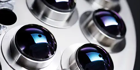
The success of the lithography process depends on several factors. On the one hand, it is possible to improve the optical properties of the wafer before applying the radiation-sensitive photoresist. Antireflection optical coating can be used to compensate for disturbing reflections. On the other hand, the success of the entire process depends on powerful optical components that enable lithography. These include high-quality systems made of lenses and mirrors.
Next-generation lithography
The generation of even smaller structures on microchips requires increasingly shorter wavelengths. EUV lithography (= extreme ultraviolet lithography) is therefore regarded as a promising successor to optical lithography. With an exposure wavelength of 13.5 nm, instead of the previous 193 nm, even smaller and more powerful microchips will be produced in the future. Among other things, extremely precise mirrors are required for the realization, which are to direct the beam path in a high vacuum. One of the greatest current challenges for the industrial application of EUV lithography is the usable power of the high-performance EUV source, as the extremely short wavelength of 13.5 nm cannot be emitted by laser. There is still a need for further research; classical optical lithography remains the main application process in the industrial production of microchips.
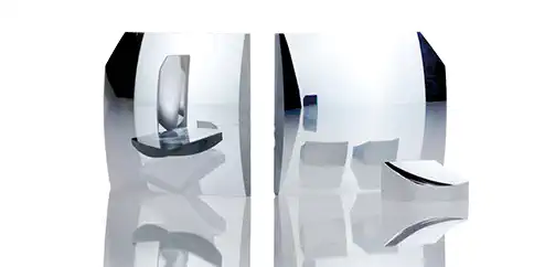
Thanks to optimized production technologies, asphericon supports you with products and services of highest quality. Low roughness lenses are one of our specialties - for minimal scattering and perfect images. Optical coatings convince by high effectiveness and longevity. Special mirrors with outstanding reflection results can also be produced - so that your lithography optics deliver the best results.
Selected product and service highlights