2-Micrometer Technology: The Key to the Next Generation of Optical Systems
Precision for Industrial and Medical Applications in the IR Range
Content
Laser technology is currently experiencing renewed momentum. In addition to the well-established 1 and 1.5 µm systems, another wavelength range is increasingly attracting attention: 2 µm (2,000 nm). Owing to its high absorption in water, distinctive interactions with materials, and the fact that this wavelength range is considered largely eye-safe, 2 µm radiation opens up entirely new application scenarios — from medicine and materials processing to sensor technology and scientific research.
This blog post takes a closer look at the unique properties of the 2 µm wavelength, its potential applications, and the challenges currently facing this technology.
Why is the 2 µm wavelength gaining attention?
The term refers to laser and light sources that emit in the spectral region around 2 µm, i.e., in the mid-infrared (MIR). Typically, these systems operate in the range between 1.8 and 2.1 µm. Unlike conventional Nd:YAG-based lasers (1.06 µm) or fiber lasers operating at around 1.5 µm, 2 µm laser technology relies on different active laser media — primarily thulium- (Tm³⁺) and holmium- (Ho³⁺) doped media. These gain media support both continuous-wave operation and the generation of ultrashort pulses with high pulse energy and excellent beam quality.
Thanks to advances in fiber technology and crystal growth processes, 2 µm lasers are increasingly reaching industrial maturity. They combine high efficiency with strong thermal stability while enabling new types of material interactions that are difficult or impossible to achieve in other spectral regions.
What is 2 µm technology?
2 µm technology refers to lasers and light sources emitting in the mid-infrared (MIR) region around 2 micrometers (1.8–2.1 µm). Typically based on thulium- or holmium-doped gain media, these systems enable precise, thermally stable processes in materials processing, medicine, sensor technology, and research. Due to strong water absorption, eye-safe operation, and new material interactions, the 2 µm wavelength range is considered a key technology for next-generation optical systems.
Distinct physical properties of the 2 µm wavelength
The 2 µm wavelength range is not arbitrary. It combines several physical advantages that make it especially attractive for a wide variety of applications and, above all, a key driver of future advances in photonics. Five selected properties are outlined below.
1. Strong absorption in water and biological tissue
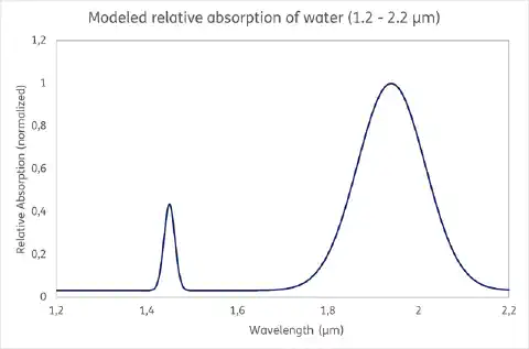
Water exhibits several strong absorption bands in this wavelength range. As a result, optical energy can be precisely deposited into tissue or other moisture-containing materials, offering a decisive advantage for medical and biotechnological applications.
Why does tissue absorb 2 µm particularly strongly?
This is because water exhibits a strong absorption maximum in the range from 1.8 to 2.1 µm. At this wavelength, optical energy is efficiently coupled into water-containing structures, enabling high-precision cutting with minimal thermal damage to the surrounding tissue.
Fig. 1: Modeled relative absorption of water in the IR range. Absorption maxima at 1.45 µm and in the range from 1.8 to 2.1 µm are particularly clearly visible.
2. Inherently eye-safe operation
Light at 2 µm is absorbed more strongly by the cornea and barely reaches the retina. This makes the technology safer and more practical for applications such as free-space optical communication and lidar.
3. New possibilities in material processing
Many materials that show little response at 1 µm behave very differently at 2 µm. These include ceramics, polymers, semiconductors with MIR transmission windows. High absorption at 2 µm for example enables improved and more precise laser processing.
4. Broad application potential for ultrashort pulses
In combination with ultrashort-pulse lasers, processes can be carried out with maximum precision and minimal thermal impact. While material absorption in conventional ultrashort-pulse systems around 1 µm is often limited, operation at 2 µm opens up additional nonlinear process windows, accompanied by modified material coupling and process dynamics.
5. Thermally stable laser sources
Thulium- and holmium-based laser systems are characterized by high beam quality (typically M² ≈ 1.1 – 1.3) and efficiencies of 30–50%. Even at elevated operating temperatures of up to about 50–60°C, beam stability and performance are maintained, making these sources particularly attractive for industrial and compact laser systems.
From medicine to microstructuring: the emergence of diverse applications
Although the technology is still in a developmental phase, a wide range of applications is already beginning to take shape.
Medicine and surgery
The strong absorption of water makes 2 µm lasers ideally suited for medical procedures. They enable precise cutting as well as targeted tissue coagulation, with minimal damage to surrounding tissue. In particular, 2 µm lasers have become established as an alternative to conventional infrared systems in fields such as urology and ENT surgery.
Material processing and manufacturing
In industrial environments, 2 µm technology enables new machining and processing approaches. Typical applications include microstructuring, cutting thin silicon layers, machining composite materials, and polymer welding.
This wavelength range is especially attractive for applications involving ultrashort-pulse lasers, as targeted energy absorption allows materials to be structured with minimal thermal effects and without the associated disadvantages of conventional processes.
Sensors, lidar, and environmental technology
2 µm technology also offers significant advantages in lidar (light detection and ranging). This wavelength is considered eye-safe while still enabling long measurement ranges. In environmental monitoring, it is used to detect and quantify trace gases such as CO₂ and methane.
Research and specialized applications
Ultrafast 2 µm fiber lasers are used in fundamental research for supercontinuum generation and to excite nonlinear optical processes. They also open up new possibilities in spectroscopy and metrology, for example in the analysis of transparent materials or thin films.
Why 2 µm lasers are the future of laser manufacturing
2 µm lasers are gaining traction because they enable manufacturing processes that were previously difficult or impractical to implement with conventional industrial laser wavelengths. They offer greater process stability when working with temperature-sensitive materials, allow for finer structural features, and support new manufacturing methods such as polymer joining, and infrared-based microassembly. As an increasing number of applications rely on precise, material-selective energy delivery, the 2 µm wavelength is emerging as a key platform for the next generation of optical manufacturing technologies.
Current challenges facing 2 µm technology
Despite its many advantages, 2 µm technology is still at an early stage of industrial adoption. The main challenges include:
- Material availability and coating optimization Not all glass or crystal materials exhibit high transmission in the 2 µm range. In addition, optical coatings must still be specifically optimized for this wavelength range, for example with respect to low absorption and high laser damage resistance.
- Thermal management The thermal conductivity of thulium- and holmium-based laser materials is lower than that of materials used at shorter wavelengths. Efficient thermal management, including controlled cooling and optimized pump geometries, is therefore crucial for stable operation.
- System integration Optical components and subsystems must be adapted to longer wavelengths, starting with fiber coupling and extending through beam shaping and delivery.
- Costs and scalability Many components are still transitioning to volume production, which means that production costs remain relatively high. These challenges highlight the need for further development before 2 µm technology can be widely adopted in industrial applications — particularly in the areas of optical components, system integration, and process stability. Several research groups and industry partners are currently working to close these gaps and make the technology suitable for large-scale industrial use.
UKPiño research project - targeted solutions for 2 µm system technology
These are precisely the challenges addressed by the RUBIN collaborative research project UKPiño. The project brings together research and development in the field of ultrashort-pulse laser applications with a specific focus on 2 µm systems. Its goal is to develop optical and mechanical designs that are jointly designed and implemented by the participating partners, including asphericon.
The project focuses, among other things, on the following components:
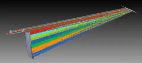
Öffner stretcher systems for stretching and shaping pulses in the 2 µm range with aberration-free precision
Fig. 3: The optimized design based on freeform optics extends the classic Öffner stretcher concept, enabling broader spectral bandwidths and improved beam quality. The transition from spherical to complex mirror geometries also allows the integration of non-interchangeable components such as gratings and high-aspect-ratio mirrors within a compact design.
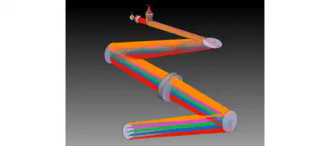
Spectral collimators for stable phase control over extended bandwidths
Fig. 4: The compact system with a folded beam path improves beam quality and ensures homogeneous illumination of the spatial light modulator. A high numerical aperture (NA) combined with sophisticated optical geometry enables precise spectral control while reducing overall system size.
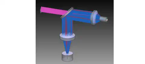
Coupling optics for efficient multi-wavelength fiber coupling
Fig. 5: A sensitivity-optimized design enables low-loss coupling of pump light from multimode fibers into active laser fibers while simultaneously collimating the laser output. High-NA aspheres, tailored coatings, and aberration compensation ensure high coupling efficiency across different pump wavelengths.
2 µm bonding lenses for focusing pulsed radiation through silicon substrates, for example in wafer bonding or microassembly
Fig. 6: Optimized for the infrared range, this system enables near-diffraction-limited focusing through silicon thicknesses of 0.25–1 mm. Carefully selected materials and coatings with high transmission at 2 µm, along with flexible system configurations, make the lens suitable for wafer bonding and microassembly processes.
These developments directly address the challenges outlined above. They improve material availability, enhance process stability, and enable optical components that previously did not exist for 2 µm applications. In this way, the UKPiño project is making a decisive contribution to the technological maturity of future MIR laser systems.
Further information on the project is available at: https://www.ukpino.com/
Outlook
In the long term, the 2 µm wavelength range offers enormous potential — not merely as a niche solution, but as a technology platform for the next generation of laser-based applications. 2 µm technology combines precision, safety, and novel material interactions within a spectral region that has so far seen limited use. Its development has now reached a point where scientific research and industrial implementation are converging. Projects such as UKPiño are actively working to bridge this gap and bring 2 µm technologies into widespread practical use.
