The laser-induced damage threshold in high-power laser optics
Causes, assessment, and how to combat it
内容
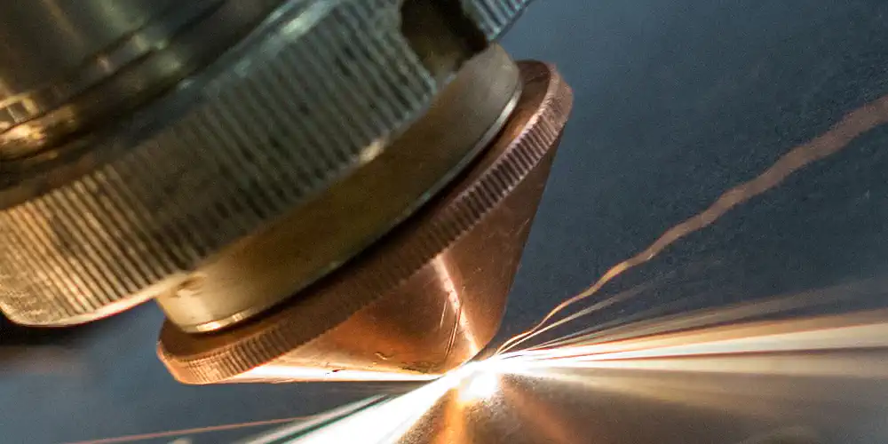
Optical components such as those found in all sorts of high-tech applications usually have a complex manufacturing chain involving several abrasive stages. During a series of machining processes, the structure or composition of the material used is abraded to produce optical substrates with high-quality surfaces and excellent characteristics. However, these manufacturing operations can also cause microscopic defects and local inhomogeneities that may lead to laser-induced damage (LID) and severely impair the performance of optical substrates under high stress. This is especially true for coated high-power laser optics if, for example, they’re irradiated at high intensity. The higher the peak pulse power they’re exposed to, the more they need to be optimized if they’re to withstand high laser intensities without suffering any damage. Lately, researchers have been exploring the causes of LID and how it can be reduced or even completely prevented.
This blog article on the laser-induced damage threshold (LIDT) will start by addressing the causes of LID during manufacture. It will then explain how this damage is evaluated and classified, and introduce ways of reducing local inhomogeneities. A second part will consider the positions and morphologies of LID, and describe the main measuring techniques used to determine the LIDT.
Does subsurface damage cause laser-induced damage?
Hard, brittle materials such as ceramics, glass and carbides are widely used in high-performance applications due to their excellent physical and mechanical properties. However, their hardness and strength make them difficult to process. Moreover, high system integrity is essential for high-power laser and lithography systems. As well as great dimensional accuracy, ultra-smooth surfaces in the low Ångström range (Angström polishing) are required.
Abbreviations
| LIDT | Laser induced damage threshold |
| LID | Laser induced damage |
| SSD | Subsurface (mechanical) damages |
| OCT | Optical coherence tomography |
| MRF | Magnetorheological finishing |
| IBF | Ion beam figuring |
| UAG | Ultrasonic-assisted grinding |
These high-performance components are manufactured using precise, deterministic machining processes, such as grinding, lapping and polishing. The snag is that each new stage may induce micro-defects and cracks in the material. Fig. 1 illustrates the manufacturing chain for optical components and the crack damage seen after each stage. Due to the brittle nature of amorphous materials, micro-defects can occur on the surface and also extend several hundred micrometres inside the material. These internal defects are referred to as subsurface (mechanical) damage (SSD). Such crack structures are particularly detrimental to the performance and lifetime of optical components and can significantly reduce the LIDT.
Fig. 1: Conventional process chain for the manufacture of optical components including close-up of the residual crack damage

The diagram in Fig. 2 shows a highly magnified view of the layer-by-layer structure of an annealed glass surface. During the polishing process, a closed layer is formed, which flows into the valleys of the roughness profile as a partly melted material, thus ‘concealing’ the SSD. This is known as the Beilby layer. It may have an amorphous or microcrystalline structure, and it consists of a highly hydrated, work-hardened material. In addition, it may contain foreign substances or impurities that can cause highly absorbent, photoactive effects. Below it is the layer of SSD (i.e. the defective layer) containing cracks up to 100µm deep. It can weaken the material and also act as a reservoir for impurities.
Fig. 2: Structure of an annealed glass surface

The type of crack paths, their depth, and the resulting surface roughness depend very much on the process parameters (cutting speed, grinding pressure, grain size and shape, grinding and polishing time) as well as on the material’s mechanical properties. Especially when it comes to high-precision applications, it’s important to quickly reach the zone of defect-free material starting from the Beilby layer. Therefore, as shown in Fig. 1, a multi-stage process consisting of pre-grinding, fine grinding, lapping and polishing with suitable parameters is usually applied during the manufacturing process. The central aim of this is to eliminate or at least reduce crack damage as much as possible in each stage. This is because the lower the SSD, the less effort will be required in the subsequent, sometimes more time-consuming steps (e.g. polishing).
Defects and SSD also affect the service life of optical coatings. These are applied to optical components after manufacturing, and enable reflection and transmission characteristics to be adapted to the specific application. However, they often suffer from serious structural defects owing to increased surface absorption during intense laser irradiation, which frequently damages the optical surface. Besides the laser damage threshold (LIDT) and the coating quality, SSD also impairs the achievable imaging quality and the mechanical properties of optical components.
Characterization of subsurface damage
With the surface integrity of optical components expected to meet ever more exacting tolerances, damage on and below the surface needs to be characterized as precisely as possible. These days, various damage detection techniques are used. As well as revealing the extent, type and position of SSD, they also provide guidance for the subsequent processing stages. These methods can be divided into non-destructive and destructive techniques. Non-destructive methods primarily include optical techniques such as microscopy, scattered light and fluorescence measurement, and white light interferometry. Other ways of gauging SSD non-destructively are prediction models and acoustic microscopy. Another promising non-destructive method is OCT (optical coherence tomography), a three-dimensional technique which delivers both quantitative information on crack depth and qualitative information on crack morphology. The diagrams in Fig. 3 illustrate how three of these methods work.
Fig. 3: Diagrams showing three different non-destructive measurement methods used to detect SSD

In addition to the above-mentioned techniques, destructive measurement methods are primarily used in industry and research. They mainly include chemical or mechanical processes, such as ion beam etching and various polishing processes. Their advantages are that they remove severe defects and eliminate residual stress in the material by means of etching and spot polishing. The polishing technique known as magnetorheological finishing is currently the preferred method for detecting SSD, and is sometimes used in conjunction with atomic force microscopy (MRF wedge technique). As well as removing residual defects, this approach also provides information about crack profiles and paths.
Processes to reduce and avoid subsurface damage
The paramount aim when manufacturing modern optics is to avoid and reduce crack structures and defects. Accordingly, various SSD-reduction methods have been developed. In particular, spot polishing processes such as MRF polishing or IBF (ion beam figuring) can be used after chemical etching to improve smoothness and LID resilience. Furthermore, special chemical process chains known as advanced mitigation processes have also been developed. The resilience of optical surfaces to laser damage can be significantly improved with a special chemical process that removes impurities and micro-cracks.
In addition, parameter adjustments and new processes during grinding have also been developed. Reduced grain sizes and UAG (ultrasound-assisted grinding) significantly diminish the depth of SSD. Moreover, hard and brittle materials have some elastic (ductile) behaviour at the microscopic level (< 1µm). If the engagement of the abrasive grains is kept within this range, ductile grinding similar to the type used on metallic materials can also be achieved for hard, brittle types of glass. This significantly lessens the formation of microcracks.
Positions and morphology of laser-induced damage
Damage to high-power laser components mainly results from abrasive processing stages during manufacture, and can arise in the material itself, on the surface of optics, or on optical coatings (see Fig. 4). Damage of this kind can greatly reduce the resilience of optical materials and coatings, and can limit the output power of laser systems. LID can have different morphologies depending on where it occurs. The most common types are listed below:
- Coating ablation: Laser damage resulting from thermally induced laser power causing blistering on coatings (Fig. 4A)
- Spot damage: occurring in dielectric materials with absorbent particles (Fig. 4B)
- Fractures and cracks: High-power laser irradiation leads to local temperature differences, resulting in strain, stress, plastic deformation, and fractures in the substrate material (Fig. 4C)
Fig. 4: Diagram showing different positions of laser-induced damage

The development and extent of damage are largely caused by thermal and electrical mechanisms, which are triggered by ambient conditions (temperature, vacuum, impurities, etc.), specific laser irradiation parameters (wavelength, pulse duration, spatial beam profile, etc.), and production-related factors. The surface and coating of optical substrates are especially susceptible to LID. Optical coating systems in particular tend to take on or even enlarge surface defects in the substrate. It’s therefore important when preparing coatings and surfaces to entirely avoid deposits or contamination. Nevertheless, the effects mentioned can also be intensified by cracks, grooves or other surface imperfections. In addition, surface roughness also affects the LIDT, which is reduced with increasing roughness.
Methods to determine the LIDT
The methods for determining the LIDT are standardized in DIN ISO 11254 and cover most laser applications. The LIDT indicates the damage threshold of a surface, as damage there is more likely than on the carrier substrate. Coatings in particular have the lowest performance in this regard. Therefore, laser optics are tested and characterized using special LIDT tests. For this purpose, either ‘destructive’ single-shot or multi-shot tests are used, in which the optics are irradiated with a defined laser peak intensity and then examined under a microscope to assess any damage. Multiple examination steps are carried out, the laser peak intensity being increased with each step. According to DIN ISO 21254, any detectable change in the sample is considered damage. The aims of this testing are to determine the operating limits and to qualify an optic for usage in a specific system. The LIDT is specified using the laser peak intensity (but note that the pulse duration used during the test must always be documented, too).
There are basically four different test methods:
- 1-on-1 test,
- S-on-1 test,
- R-on-1t est
- Raster scan test
They are explained below.
1-on-1-test
The 1-on-1 test (an ISO-certified LIDT test) is ideal for optimizing manufacturing processes. It’s also regarded as a simple, easy-to-interpret method for determining the LIDT. To carry out the test, the sample surface is subdivided into a matrix or test pattern of spatially separated test sites (cf. Figure 5), which is then irradiated once by a laser with a preselected pulse energy and laser peak intensity. After each pulse, the energy and the condition of the irradiated site are recorded. The sample is examined to identify any damage, and then the probability of damage is calculated. This process is repeated for all other sites while increasing the pulse energy until the damage probability reaches 100%. According to DIN ISO, the threshold equates to the highest amount of laser radiation hitting the optical surface for which the extrapolated (i.e. estimated) probability of damage is zero. The calculation of the LIDT is carried out using suitable extrapolation models and corresponds to an estimate as a function of the pulse energy applied produced.
Fig. 5: Diagram of the 1-on-1 test

S-on-1-test
In contrast to the 1-on-1 test, the S-on-1 test comprises multi-shot testing. Once again, the surface of the sample is divided into a defined matrix with spatially well-separated test sites. However, instead of being irradiated with a laser pulse just once, the test sites are irradiated with a high number of laser shots of the same intensity (usually between 10 and 1,000 shots with a low repeat rate). As in the 1-on-1 test, the intensity is increased with each new test sequence. To determine the LIDT, the number of pulses applied before damage occurs is recorded and used to evaluate the LIDT as a function of the number of pulses. If damage occurs during the test, irradiation is halted to prevent further damage to the sample. The high flexibility of this test method is advantageous because different pulse repetition rates can be applied. In addition, this method provides a significantly more accurate prediction of the actual performance of the optics, which is why the S-on-1 test is the method of choice when it comes to determining the exact LIDT. A practical damage curve is produced showing the energy density values for selected damage probabilities as a function of the number of pulses.
Fig. 6: Diagram of the S-on-1 test

R-on-1-test
Unlike the first two test methods, the R-on-1 test isn’t an ISO-certified test. The main difference is that it’s a ‘ramp test’ in which just one area of the sample is irradiated, the laser intensity being gradually increased until damage occurs (see Fig. 7). This method is very time-consuming because the principle has to be repeated for a large number of test sites depending on the size of the sample and the size of the laser spot; moreover, the same initial intensity has to be used each time. In addition, the damage intensity isn’t determined by extrapolating the damage probability as in the ISO-certified tests. Instead, the highest fluence level at which the damage probability is zero is taken as the LIDT. Furthermore, to ensure the highest possible accuracy, the ramp gradations should be made as small as possible.
Fig. 7: Diagram of the R-on-1 test

Raster scan method
Although the raster scan method isn’t ISO-certified either, it’s increasingly being used due to the growing demands on optical components. It uses much larger spot diameters (1 mm scans 1 cm²), resulting in overlaps and enabling a larger proportion of the surface to be tested. Accordingly, this method is also suitable for large-area optics, since even rare defects can be pinpointed. The performance of a sample is determined by carrying out a multiple pulse raster scanning procedure. Scanning is analogous to the R-on-1 test method in that a point on the sample is irradiated and the fluence steadily increased until damage occurs. The difference is that the LIDT corresponds to the intensity at which ten or more damage events are observed.
Fig. 8: Diagram of the raster scan test

LIDT in high-power laser optics - Summary
The blog article on the LIDT sheds light on the complex production chain required for optical substrates with high surface qualities and performance properties, which are particularly essential for high-power laser components. However, these manufacturing steps can induce microscopic defects, inhomogeneities and SSD that impair laser optics in terms of their coating quality, mechanical properties and resilience to laser damage. There is clearly great interest in reducing such damage. Especially when used in highly sophisticated laser applications, damage can occur in a wide variety of places and morphologies. Since this damage is partly related to the laser peak intensity, various single-shot and multi-shot tests are used to determine the LIDT when specifying laser optics. The LIDT enables the selection of optical components for specific applications with a view to preventing their rapid wear.