Optical coating methods
Modern optical coating processes
内容
After introducing the field of optical coating, e. g. via filter and anti-reflective coatings, beam splitter and dielectric mirrors, the following article shows how to obtain the coating materials with the desired properties on optics made of glass, metal or other materials. Optical coatings are used in a variety of applications, including:
- Components for highly demanding laser applications (low scattering, high reflection, high laser damage thresholds), ultra-short laser pulses
- Demanding environmental conditions, e.g. high temperature fluctuations, high cleaning requirements (e.g. space applications)
- Filter and beam splitter for imaging and the semiconductor industry
- HR Coatings for life sciences and photonics
Optics production offers various technologies for the optical coating process. The choice depends on the properties of the raw material and the specifications of the optical systems/products. The most common coating technologies for high performance optical components include:
- thermal vaporization and
- sputtering technology
Thermal deposition for a high-performance surfaces
Thermal deposition (EBE – Electron Beam Evaporation) is the most common and oldest optical coating process for coating optical substrates. During evaporation, the materials are evaporated in a vacuum chamber at 10-4 mbar either by high temperatures or by knocking out with an electron beam. The adequate optical coating process is selected depending on the material properties (e. g. melting point) and the optical specification. The material to be evaporated is located in a suitable container or in so-called boats at the bottom of the vacuum chamber. By current flow or an electron beam it is brought to its boiling temperature and evaporats. Since the vapour particles propagate almost linearly in a high vacuum without collision, they condense evenly when they hit an obstacle. The optical substrate to be coated is located on a rotating calotte in the upper part of the evaporation chamber (figure 1). Control of temperature, vacuum pressure, substrate position and rotation during vaporization ensures uniform optical coating of a certain thickness.
Advantages of evaporation
- Variety of coating materials
- Flexibility of the substrate shape
- High quality anti-reflective & metal coatings
- Best cost-benefit ratio
In addition to EBE, a plasma source is used in asphericon’s coating systems. This ion-assisted deposition (IAD) ensures that the growing layer is additionally compressed by a plasma bombardment. The result is a harder, more stable layer.
Before the optical coating process starts, the lenses of course have to be thoroughly cleaned manually or by ultrasonic washing to remove impurities, such as dust, and to prevent functional impairment. The properties of the applied layer can also be specifically modified by means of a heat treatment, so-called tempering. This last refinement is achieved by heating the lenses, which removes the water from applied layers. The advantage of this additional process is the further optimization of the coating of optics. However, only certain coating materials can be tempered.
Figure 1 Schematic representation of the evaporation process
Sputtering: Hard layers of high climatic and mechanical stability
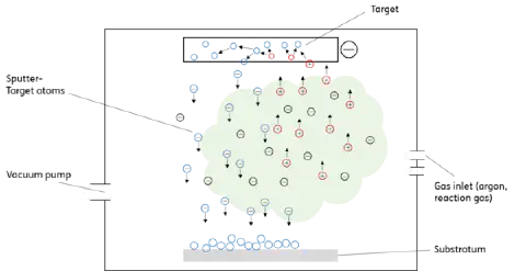
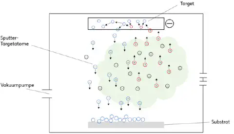
In coating technology, sputtering refers to the removal of particles (e. g. atoms) from a solid target. For this purpose, high-energy ions are generated in a plasma in a vacuum and accelerated in the direction of the target by an external electric field. The ions collide with the atoms of the target and form impact cascades. If a minimum energy of about 20eV is exceeded, the target material is removed. Some of the particles (target atoms) leave the target and move towards the substrate, where they are deposited as a thin layer.
The use of this optical coating process is suitable for optics in a wide wavelength range and can be divided into different types, which are mainly distinguished by the ion source used:
- Plasma sputtering
- Ion beam sputtering
Advantages of sputtering
- Mechanically very stable optical coatings
- Lower coating temperature
- Suitable for demanding dielectric filter and HR layers as well as laser applications
Plasma sputtering – Optical coating by gas discharge
Plasma sputtering encompasses various optical coating processes such as magnetron, DC and RF sputtering. The common feature of these processes is the recovery of ions by gas discharge. A plasma is ignited by applying a voltage and introducing noble gases (usually argon). This releases ions which hit the target with high kinetic energy and, thus, dissolve sputtering target atoms from the surface.
Magnetron sputtering uses a magnetic field that forces the electrons in the vicinity of the target to move in a spiral motion along the target surface. This process can be used to produce hard and mechanically resistant optical coatings.
A DC voltage is applied for DC sputtering, whereby the target forms the negative electrode and the substrate the positively charged electrode. The positive (argon-) ions from the plasma hit the target and dissolve target atoms through shock cascades, which deposit on the substrate. Only conductive targets, such as metals, can be used for this process.
RF sputtering is a high-frequency alternating field that alternately accelerates the (argon) ions and electrons of the plasma in both directions. In plasma, the high-energy electrons reach free surfaces faster than the ions. This means that each surface is negatively charged against the plasma and thus develops a self-bias. In this method, argon ions are also accelerated to the solid target (cathode) and knock out atoms. Since the positive charges do not have to be discharged, non-conductive materials can be atomized.
Ion beam sputtering (IBS): For denser layers with low reflection
IBS uses a distinct ion source separated from the target and substrate. Heavy monoenergetic ions (e. g. 40AR) are generated, focused and shot vertically at the targets to be atomized at energies of typically 5 to 20 keV. The ions hit the target surface and, thus, trigger the sputtering target atoms, which condense as a dense coating on the substrate. The attainable film thickness on the substrates depends on the ion flow, the distance between substrate and target, the angle between holder and target surface and the atomization time.
Figure 2 Schematic diagram of IBS
Compared to MS sputtering, the IBS coating process is technically more complex, therefore above all more cost-intensive, and is primarily suitable for selected, extremely demanding coating systems.
Thanks to many years of experience and state-of-the-art technology, asphericon supplies high-quality optical coatings according to your specifications. Coatings in the spectral range from ultraviolet (190 nm) to mid-infrared (5 µm) can be realized. Find out more about our coating services or contact us directly to learn more about custom optical coatings for a wide wavelength range.
From optical design to the selection of the right coatings for your products, we would be happy to support you.


